

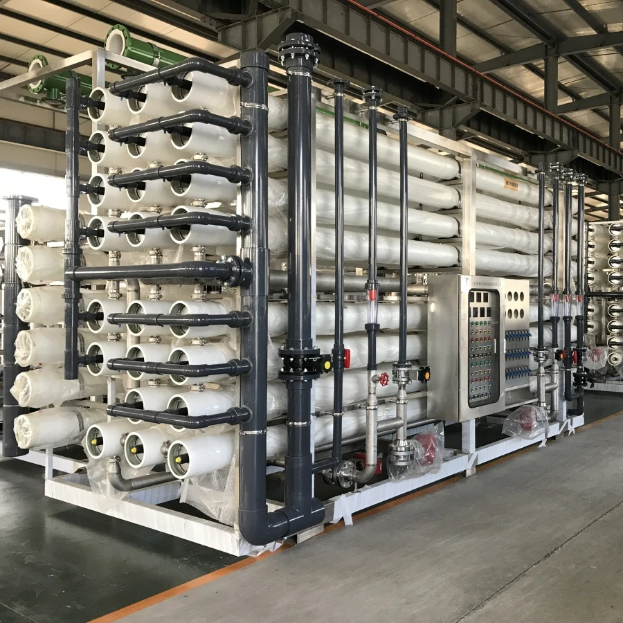


Reverse Osmosis System in the Semiconductor Industry
Reverse Osmosis System in the Semiconductor Industry: Critical for Water Purity and Process Precision
The semiconductor industry, which underpins the modern digital economy, requires highly precise manufacturing processes, where even minute variations in material purity and environmental conditions can significantly impact product quality and yield. One of the most critical factors in semiconductor fabrication is the purity of water used in various stages of production, including cleaning, etching, and rinsing processes. Semiconductor reverse osmosis (RO) systems have become indispensable in ensuring the quality of water that meets the stringent requirements of semiconductor manufacturing.
The Role of Reverse Osmosis in Semiconductor Manufacturing
Semiconductor manufacturing involves several stages where water plays a vital role, including wafer cleaning, photoresist development, etching, and chemical mechanical planarization (CMP). In each of these steps, ultrapure water for semiconductor manufacturing must be of extremely high purity to avoid contamination that could degrade the final product. So water treatment in the semiconductor industry plays a significant role. Here's how semiconductor reverse osmosis systems contribute to each of these critical stages:
Wafer Cleaning and Rinsing: One of the most essential steps in semiconductor fabrication is cleaning the wafers to remove dust, organic material, and any residual chemicals from previous process steps. Ultra-pure water Reverse Osmosis system ensures that no impurities are introduced during this delicate stage. Any contamination on the wafer surface could cause defects in the thin film deposition process, leading to failures in the final device.
Etching: Etching is used to create patterns on the semiconductor wafer by removing layers of material. Impure water could introduce unwanted ions or organic substances that might react with the wafer's surface, compromising the quality and precision of the etching process.
Chemical Mechanical Planarization (CMP): CMP is a critical process in semiconductor manufacturing that involves polishing the wafer to ensure a flat and uniform surface. Water is used to rinse the wafer and remove slurry and particles during this process. RO water, which is free of minerals, ensures no undesirable residues remain that could interfere with subsequent layers of deposition.
Photolithography: Photolithography is used to transfer patterns onto the semiconductor wafer. The process involves a photoresist material that is sensitive to light, and the purity of water is important in washing away any particles that might interfere with the fine patterning. Contaminants, even at very low concentrations, can cause defects or even complete failure of photolithographic processes.


Hot Tags: semiconductor reverse osmosis system, China semiconductor reverse osmosis system manufacturers, suppliers, reverse osmosis desalination, Commercial ro water purifier, water world ro systems, seawater reverse osmosis, water softener system with reverse osmosis, reverse osmosis machine price